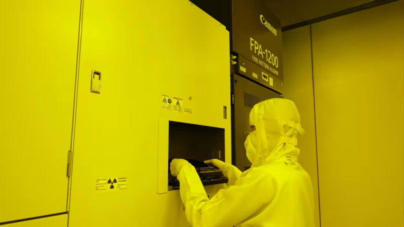
Canon hopes to start shipments of new low-cost chip-making machines as early as this year, as the Japanese company best known for its cameras and printers tries to undercut longtime industry leader ASML in providing the tools to make leading-edge semiconductors.
The challenge from Canon comes as Western governments attempt to restrict China’s access to the most advanced semiconductor technologies and as global demand for chipmaking machines has soared. If successful, Canon’s “nanoimprint” technology could give back Japanese manufacturers some of the edge they ceded to rivals in South Korea, Taiwan and, increasingly, China over the past three decades.
“We would like to start shipping this year or next year... we want to do it while the market is hot,” said Hiroaki Takeishi, head of Canon’s industrial group, who has overseen the development of the new lithography machines. “It is a very unique technology that will enable cutting-edge chips to be made simply and at a low cost.”
First unveiled in mid-October, Canon’s nanoimprint lithography—a technology under development for more than 15 years but which the company says is only now commercially viable—stamps chip designs onto silicon wafers rather than etching them using light.
The process, says Canon, will be “one digit” cheaper and use up to 90 percent less power than Netherlands-based ASML’s market-dominating and light-based extreme ultraviolet (EUV) technology.
Competitors have been progressively outflanked by ASML, the only group able to make the highly sophisticated EUV machines vital to the production of the latest generations of chips at manufacturers such as Taiwan Semiconductor Manufacturing Company, Samsung Electronics in South Korea, and Intel in the US.
But the machines made by the Dutch tech company are also the most expensive part of the manufacturing process, costing more than $150 million each, and there are long lead times for delivery, giving Canon some space to market its technology.
“Our objective is not to grab share away from EUVs... but we believe our nanoimprint technology can coexist with EUVs and other technologies and contribute to the overall growth in the industry,” Takeishi said.
Although Canon is optimistic it can carve out a niche—focusing first on 3D Nand memory chips rather than more complex microprocessors—analysts are skeptical of the impact it can make.
“This tech is nothing new... if nanoimprint technology was a superior technology, I think it would have been up and running by now and in the market in volume,” said Richard Windsor, founder of research company Radio Free Mobile.
One of the biggest challenges for Canon is increasing its success rate in achieving greater levels of miniaturization. It is starting at the 5-nanometre—or billionths of a meter—node for circuit widths and is aiming to reach 2nm.
Takeishi would not be drawn on the potential yield—the proportion of chips produced that are deemed flaw-free and shippable to customers—from the nanoimprint machines, but analysts have said it would need to be near 90 percent to compete with EUV.
“In regards to defect risk, I think our technology has largely resolved the issue,” Takeishi said. “But since the existing chip manufacturing processes are optimized for EUVs, there will obviously be various difficulties in terms of bringing in new technology.”
The first deliveries will therefore be for trial periods, with Canon having to convince customers that the effort of integrating the new machines into existing fabrication plants is worthwhile. The company said major layout changes would not be necessary, but some extra equipment such as cleaning machinery and for mask production would be needed.
One hope of analysts had been that Canon might be able to sell the machines to China, something ASML can no longer do with its advanced tools due to US export controls. However, Japan’s own export controls, designed to align with Washington, target advanced semiconductor manufacturing equipment more broadly, making it difficult for Canon.
“There aren’t that many options left but to pay careful attention to this issue,” Takeishi said when asked how much the company considered the risk of sanctions in developing the nanoimprint lithography machines. “It’s come to a point where nobody knows where the risks are.”
© 2024 The Financial Times Ltd. All rights reserved. Not to be redistributed, copied, or modified in any way.
Reader Comments (118)
View comments on forumLoading comments...